PCB-design på Kicad 8
IDA supports the UN's world goals
IDA wants to make visible the link to the United Nations 17 Sustainable Development Goals (SDG). This event covers, among other things, the above development goals. Read more about the UN's 17 Sustainable Development Goals (SDG)
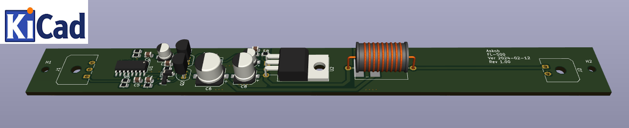
Med udgivelsen af Kicad 8 er der igen sket en del på opensource PCB-designfronten. Vi skal se på, hvordan man designer PCB. Vi vil designe et print og få det lavet. I vil derefter efter ca. en uge kunne hent jeres PCB.
With the release of kicad 8 a lot have happen in the field of PCB design. We will look at:
- Main KiCad window (project window)
- Schematic editor
- Symbol library manager
- Simulator
- Schematic setup
- Symbol properties
- Symbol editor
- Layout editor
- Layout editor setup
- Footprint properties
- 3D viewer
- Gerber viewer
- Image Converter
- Calculator tools
- Drawing sheet editor
- Plugin and content manager
The presentor is Gert Lauritsen, who've been designing PCB for 25+ years.
IDA supports the UN's world goals
IDA wants to make visible the link to the United Nations 17 Sustainable Development Goals (SDG). This event covers, among other things, the above development goals. Read more about the UN's 17 Sustainable Development Goals (SDG)
This event is closed for registration.
Information